Fostering innovation

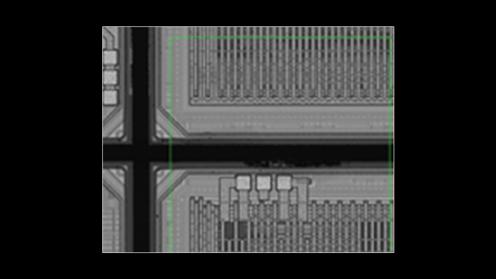
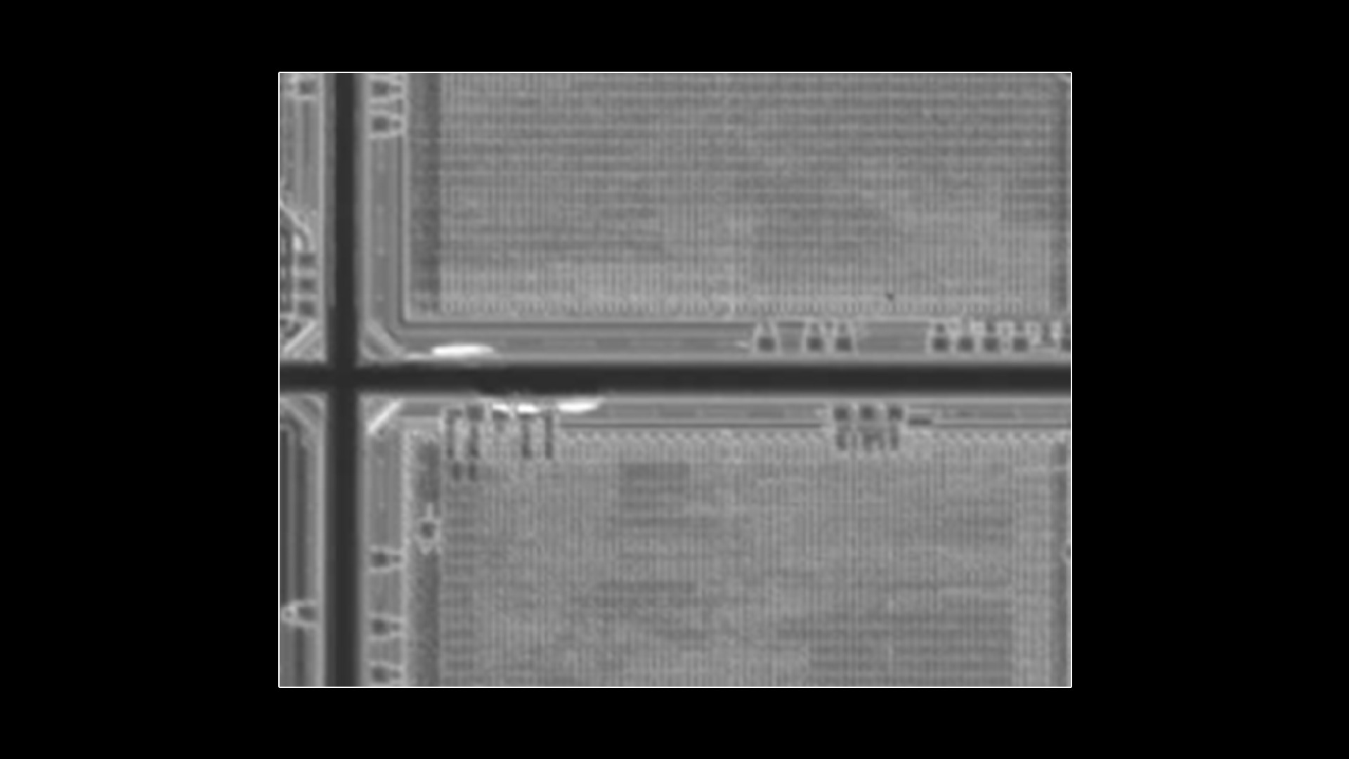
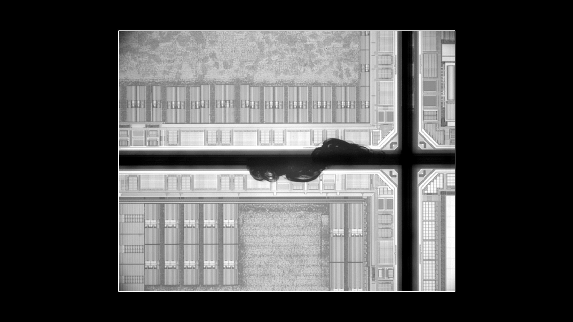
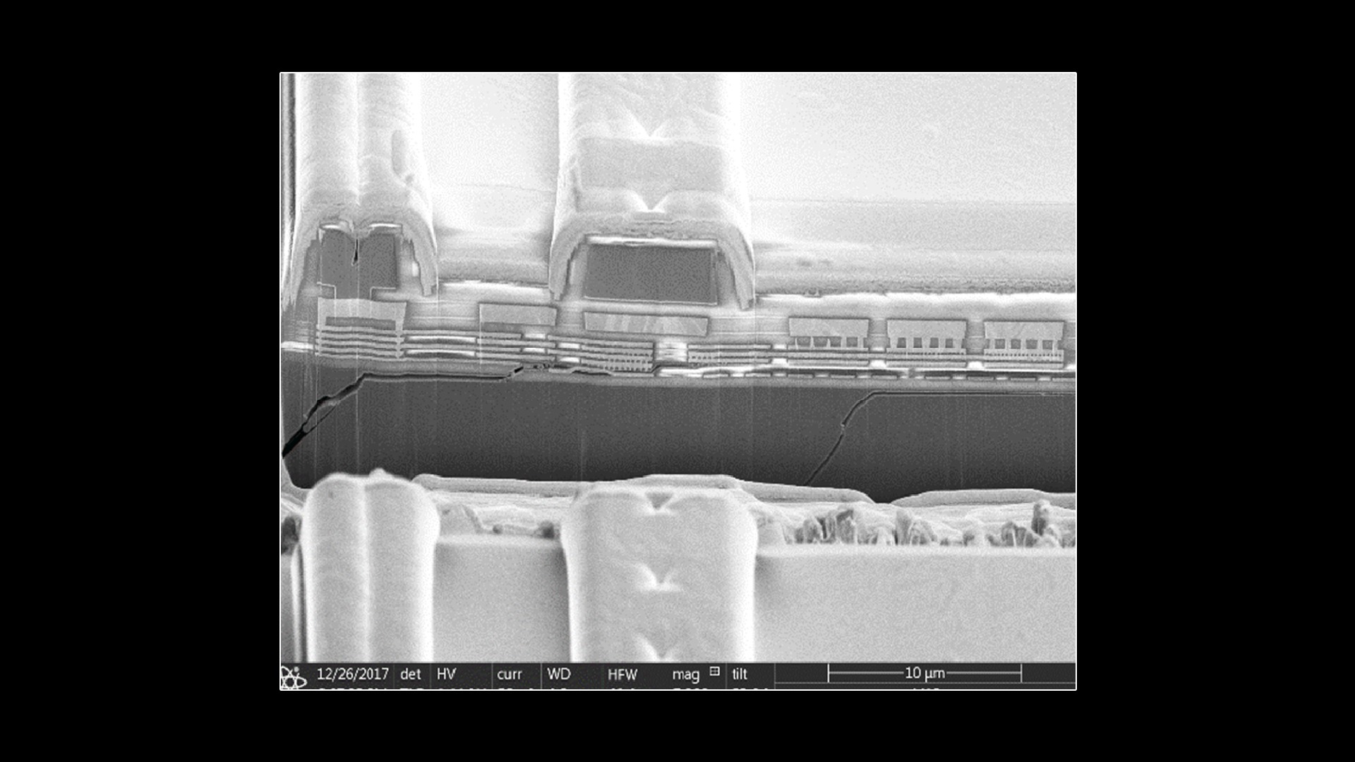
Inner Crack Imaging
The detection of inner cracks, or side wall cracks, that occur during the dicing process and are not visible to standard inspection and testing techniques is crucial. These cracks can ultimately cause failure in end-products or mission critical systems, such as in the automotive industry, resulting in significant losses to the manufacturers of the end user devices.
While IR inspection is taken from the backside, requires pre-preparation and is not production worthy (up to 5 hours for a full wafer scan), Camtek’s pioneering Inner Crack Imaging (ICI) technology enables the detection of inner cracks during wafer level inspection, immediately after dicing in a high-volume production environment.
Highlights
- A unique patented technology combining hardware (optics) and SW solution
- High accuracy rate for inner crack detection
- High productivity - Full wafer scan @ less than 3 minutes.
- ICI technology can be deployed on Camtek’s Eagle products family
- Upgradable
- Scanning for inner cracks can run as an additional recipe together with standard surface inspection
- Easy set up
- Simple classification for inner crack candidates
Products