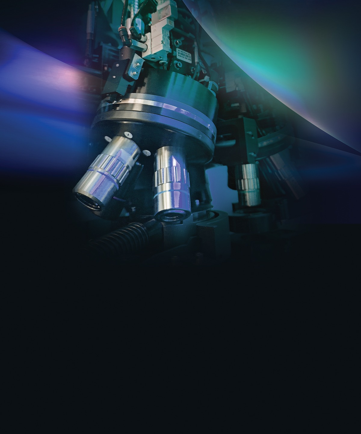
Macro Inspection

Detecting typical defects of interest at full production rate
With geometries getting smaller, Back-end-of-Line (BEOL) of the Front-end inspection becomes both more challenging and crucial for defect-free and high-yield wafer manufacturing. The variety of defects calls for detection optimization, fast screening and categorization of the high volume manufacturing environment, while maintaining high throughput.
BEOL of the Front-end inspection challenges vary from one process step to another, and include:
- In the lithography process step, defects of interest include: Defocus, bad coatings, blocked contacts, bridging, missing or extra patterns and critical dimension variation;
- In the etch process step, defects of interest include: Particles, pinholes, peeling, residues, water marks, scratches and corrosion;
- In the chemical mechanical polishing (CMP) process steps, defects of interest include: Scratch detection, residue detection, unpolished/insufficiently polished areas and brush marks;
- In the outgoing quality control (OQC) process step, defects of interest include: particles, pinholes, peeling, residues, water marks, scratches and corrosion.
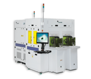
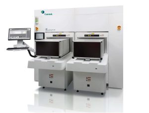
Camtek’s Eagle platform can handle all these challenges and detect typical defects of interest at full production rate.
Capabilities
- Full coverage inspection providing zero PPM to the most advanced technology nodes
- Enhanced 2D detection algorithms with color variation robustness
- Sub-pixel alignment mechanism
- Backside inspection, including: Modular backside unit, detection of macro cracks, scratches, contamination and wafer chippings
- High throughput in high-volume manufacturing rate
- Combined dark and bright field illumination
- Capability to merge front side inspection and back side inspection results
- Creating recipes offline maximizing tool utilization
- Analytic tools, including Automatic Defect Classification (ADC) and yield management system
Products
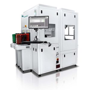
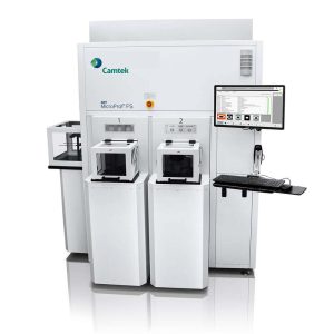
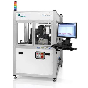
MicroProf® MHU
Material Handling Unit with dual-arm robot for the semiconductor, MEMS, and LED industries
Learn More >