MEMS

Unique flexible platform supporting the entire spectrum of MEMS applications
The Micro Electro-Mechanical Systems (MEMS) market is changing and growing, driven by the increased number of sensors in consumer electronics like smartphones and technical innovations in the automotive industry. Connected devices that use sensors include cars, wearable technology, home products, and more.
Optical MEMS inspection has a two-fold challenge. The multiple levels and areas of interest all require careful inspection at high speed. Additionally, special handling is required for wafers with sensitive areas, such as membranes. Inspection requires the ability to process and evaluate a large variety of wafer types and sizes, up to 8 inches.
Camtek’s inspection and metrology solutions for MEMS combine variety of technologies for addressing the 2D and 3D challenges of the MEMS industry.
Our unique flexible platform supports the entire spectrum of applications within the MEMS industry. Several forms of handling configurations and special developments are available to support the various wafer sizes and types.
Capabilities
- 100% wafer inspection and 2D metrology
- Surface-related defect inspection
- Various handling solutions
- High-resolution 2D and 3D measurement
- Multiple illumination configurations for inspection of various features
- Flexible detection environment for customized applications
Technologies
- Advanced detection engines for defect inspection and metrology
- High-resolution 3D confocal sensor and white light interferometer
- High-intensity back-light LED illumination, enabling the detection of defects that cannot be seen with regular BF or DF illumination

Products
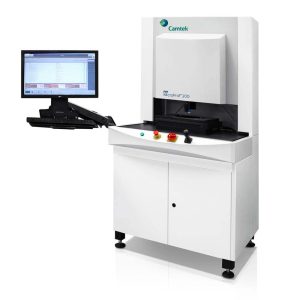
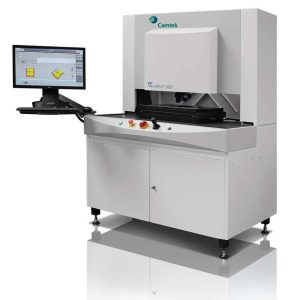
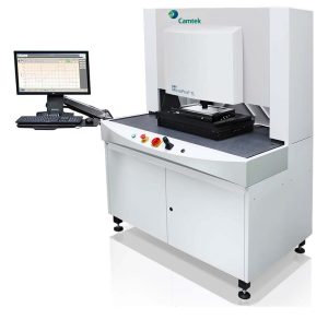
MicroProf® 300
Powerful metrology tool for quality assurance, development and manufacturing
Learn More >
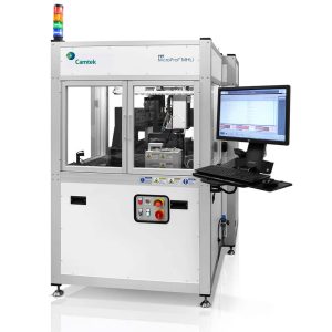
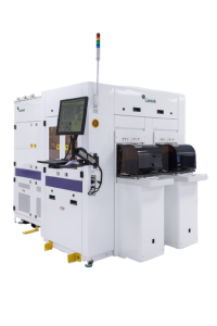
MicroProf® MHU
Material Handling Unit with dual-arm robot for the semiconductor, MEMS, and LED industries
Learn More >