Post Probing Inspection

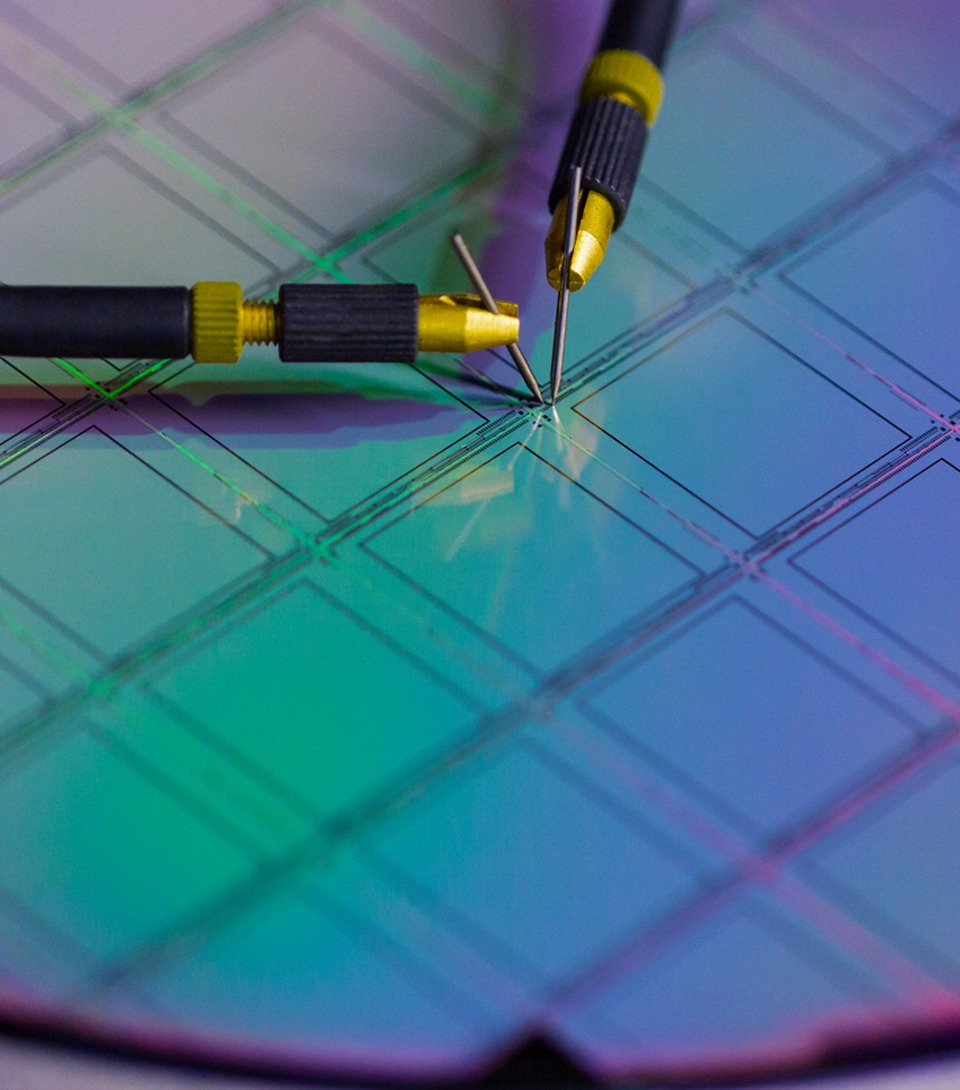
Detecting and measuring damages caused during wafer probing
Most wafers undergo the wafer sort process in which each device (or die) is tested electrically to assure its functionality. This process is based on a matrix of needles that physically touches the device input/outputs, thus enabling the electrical test. The actual probing of the dice by the needles may cause some damage.
Camtek offers advanced inspection and metrology solutions to detect and measure damage caused during the wafer probing process. Our solutions were developed to address a variety of defects critical to device quality while also providing analysis to enhance production and yield.
Our post-probing inspection offering is an integral part of our general surface inspection solutions designed to support a high-volume production environment.
Capabilities
- Detection of miniature passivation cracks
- Detection of damage on probed bumps
- Detection and measurement of probing process issues, such as probe needle mark shift, probe needle mark size,
- Advanced analysis tools, including unique 3D sensors for the analysis of probe needle mark depth
- High throughput for 100% inspection
- A variety of reports and charts for process control and analysis
Technologies
- Advanced processing engines for defect inspection and metrology
- High-resolution 3D confocal sensor and white light interferometer
- Statistical analysis of probe mark size, proximity and anomality
Products
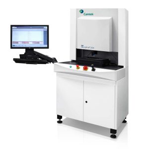
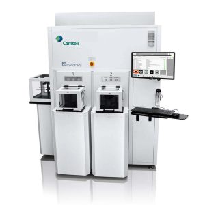
MicroProf® 300
Powerful metrology tool for quality assurance, development and manufacturing
Learn More >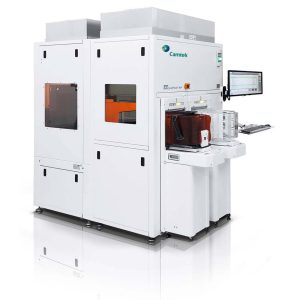
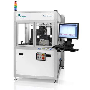
MicroProf® MHU
Material Handling Unit with dual-arm robot for the semiconductor, MEMS, and LED industries
Learn More >