Un-patterned Wafers

The ideal for the inspection of EPI wafers
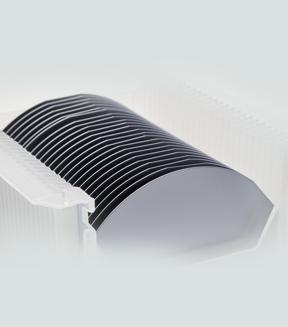
Un-patterned wafers inspection is becoming more critical due to the need to find defects earlier in the manufacturing process flow. Finding those defects is getting harder as critical dimensions shrink. Un-patterned wafer inspection looks for defects on unprocessed or bare silicon wafers.
Inspection challenges are numerous and include accurate defect position reporting, wafer warpage monitoring, 3D defect identification, shallow defect detection, wafer surface quality monitoring and fully automated data collection. Camtek solutions address all these challenges providing a total solution in one tool, including yield prediction capabilities, scanning or profiling defects based on bin code and analysis of 3D issues based on a 2D scan. Together with high throughput in full production rate, our solutions are ideal for the inspection of EPI wafers.
Capabilities
- Feature-based defect classification
- Wafer edge alignment
- Special wafer placement confocal sensor for bow measurement
- Unique optics detecting topography deviation in high throughput
- Dedicated optics allowing fast slip line detection combined with image processing
- Dedicated algorithm combined with slip line optics for fast wafer surface quality inspection
Technologies
- Surface Topography Sensor
- New light channel for slip line detection
- Yield prediction
- Flexible profiling capability based on bin/die
- Deep learning based classification
Products
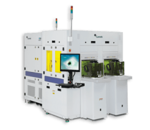
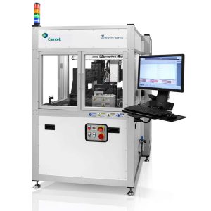
MicroProf® MHU
Material Handling Unit with dual-arm robot for the semiconductor, MEMS, and LED industries
Learn More >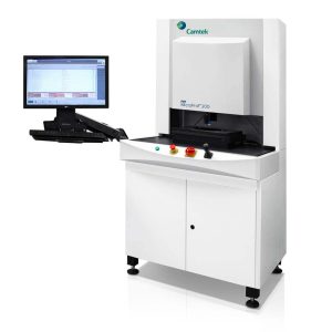
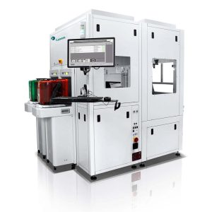
MicroProf® 300
Powerful metrology tool for quality assurance, development and manufacturing
Learn More >