Post Dicing
Post Dicing
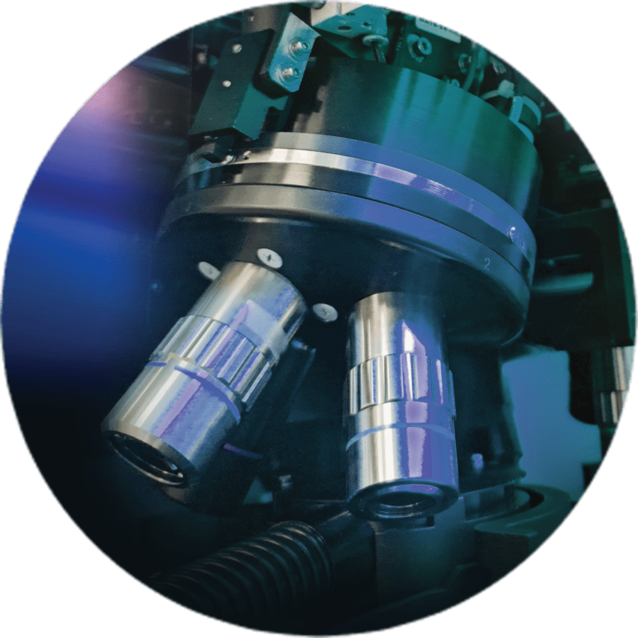
Camtek offers dedicated inspection and metrology solutions for dicing-related processes, ensuring the reliability of the end product. Camtek developed new capabilities to address new dicing technologies such as Stealth and Plasma dicing using new algorithmic and technologies such as Back Light illumination, as well as various handling solutions.
Our multi-level software alignment capability precisely aligns each die with its reference, ensuring reliable detection for diced, stretched and reconstructed wafers. Camtek provides a variety of handling configurations that cover various wafer sizes and types and a quick setup, in line with the demanding high-volume manufacturing environment.
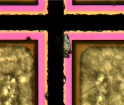
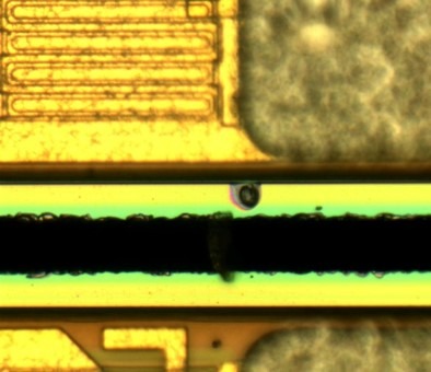
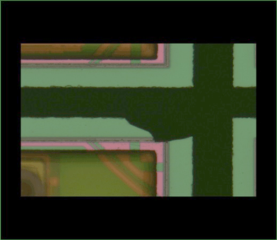
One of the killer defects in post diced wafers, mainly with low-K materials, is side wall cracks. However, the detection of these cracks has been historically challenging. Camtek has developed a unique technology for the detection of side wall cracks. In the emerging advanced packaging market, the detection of these cracks in the early process stages is crucial for a defect-free end product, saving the whole manufacturing chain undesirably high costs.
Capabilities
- Detection of sub-micron surface defects
- Dedicated algorithm for chipping inspection to ensure die integrity
- Kerf metrology and inspection, both chip in and out
- Die boundary violation, such as oversize die
- Micro and side wall cracks
- Real time die alignment
- Simultaneous detection of die active area and street
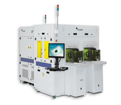
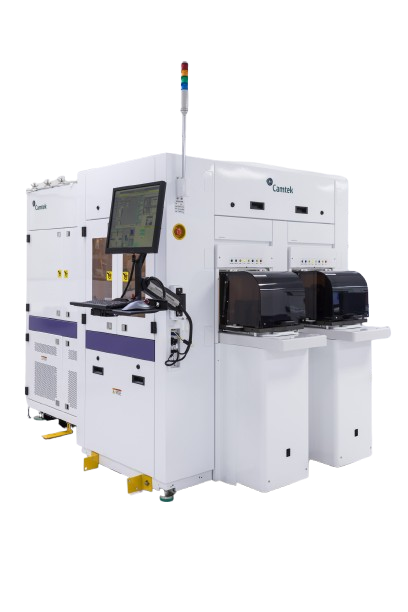
Products