Products
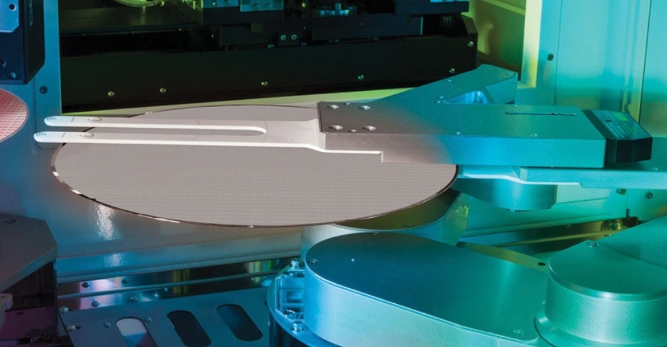
Camtek offers a wide range of full wafer Inspection and Metrology solutions for the Semiconductor industry. Our inspection and metrology systems can detect defective ICs reliably at high-throughput, ensuring that only known-good-dies are delivered to our customers’ final products.
BEOL of the Front-end
Camtek’s Eagle platform can handle the many challenges of macro inspection and detect typical defects of interest at full production rate.
Learn More >
Advanced Packaging
With years of experience in the advanced packaging market and partnerships with the world’s leading manufacturers, Camtek’s combined 2D and 3D inspection and metrology platform is the industry standard for sampling and high-volume production environments.
Learn More >
Post Dicing
Dedicated inspection and metrology solutions for dicing-related processes addressing new dicing technologies such as Stealth and Plasma dicing.
Learn More >
Silicon & Compound Wafers
The compound semiconductors manufacturing process is unique and requires dedicated solutions for Inspection and Metrology. Camtek’s offering includes the inspection of Epitaxial layers, inner cracks within the Epitaxial layer, surface topography, Bow measurement, data analysis and more.
Learn More >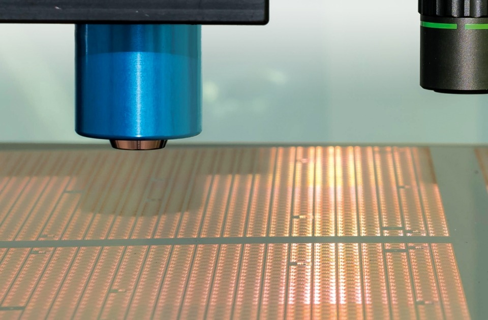
Panels
Designed mainly for Fanout Panel-Level-Package (FO-PLP) applications, Camtek’s Golden Eagle is used for the inspection and metrology of standard panel sizes, up to 650mm x 650mm.
Learn More >