Fostering innovation

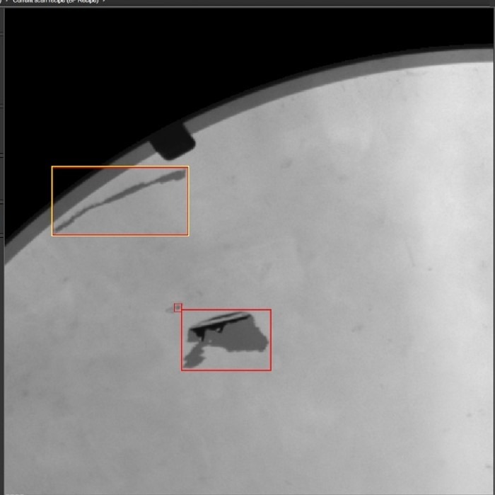
Backside Inspection
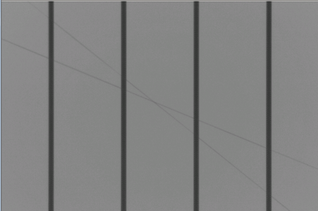
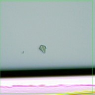
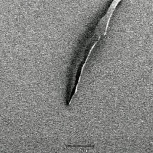
Inspection of the wafer’s backside has become valuable, assuring wafers have not become contaminated with particles or damaged, which eventually results in yield loss.
One of the main challenges of backside inspection is enabling the inspection of wafers’ backside on the same scan without compromising on throughput.
To meet these challenges, Camtek’s Eagle platform provides integrated backside inspection capabilities enabling the inspection of wafers (bare or framed) back side in two different modes:
- Macro (BSI) – low resolution defects, no impact on throughput
- Micro (Flipper) – high resolution defects (0.5um)
Highlights
- Modular Backside unit (8” and 12” wafers)
- Detection of macro cracks, scratches, contamination and wafer chippings
- High volume manufacturing rate
- Combined dark & bright field illumination
- Front side inspection and back side inspection results are merged into a single report
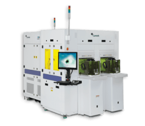
Products