Silicon & Compound Wafers
Silicon & Compound Wafers
Compound semiconductors are undergoing a major expansion addressing many new applications and using various materials such as SiC, GaN, GaAs and others, to improve the performance of new devices in several segments such as Power and Face Recognition.
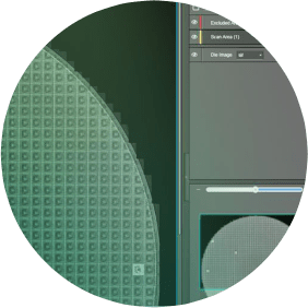
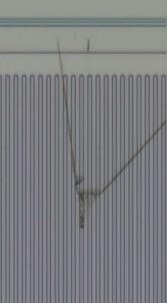
The compound semiconductors manufacturing process is unique and requires dedicated solutions for Inspection and Metrology. Camtek’s offering includes the inspection of Epitaxial layers, inner cracks within the Epitaxial layer, surface topography, Bow measurement, Slip Line inspection, data analysis and more.
Capabilities
- Small defect detection at high resolution
- Inspection of transparent wafers
- Metrology, including wafer bow measurement, surface topography
- Inspection – epitaxial substrate
- Line process
- Data analysis
- Yield prediction

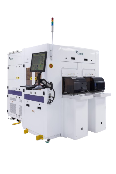
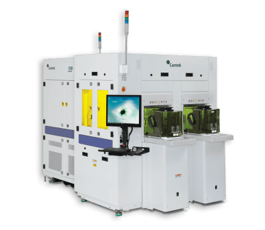
Products