Advanced Packaging

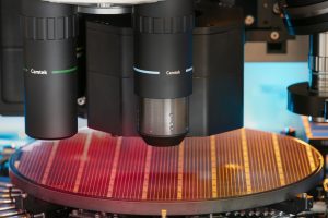
Combined 2D and 3D inspection and metrology
Growth in the advanced packaging market and the challenges raised by the various packaging types requires the highest level of inspection and metrology, ensuring high yields of each die as well as of the whole package.
With years of experience in the advanced packaging market and partnerships with the world’s leading manufacturers, Camtek’s combined 2D and 3D inspection and metrology platform is the industry standard for sampling and high-volume production environments.
Inspection challenges:
- Scanning the whole wafer’s surface conditions, including front side, back side and edges
- Attaining zero parts per million defect levels
- Detection of defects ranging from microns to sub-micron
- Highest throughput for 100% inspection
Metrology challenges:
- Increased I/O density
- Huge amount of I/Os
- Wide range of bump height
- Bump type variety
- Bump metrology on Multi RDL layers
- Bump top Morphology
Sub-micron defect detection powered by advanced algorithms
Computer Aided Design-based detection technology
Clear sight inspection for multilayer redistribution layer (RDL) applications
Inner Crack Inspection (ICI) for post-diced wafer
Backside inspection
Backlight illumination technology
100% and sampling bump measurement at the highest throughput
Down to 2µm redistribution layer (RDL) thickness
Critical dimension/overlay of any object type and size
- True die shift position
- EBR metrology and defect inspection
- Auto setup/calibration
- High- and ultra-high throughput configurations

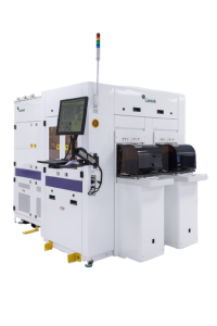
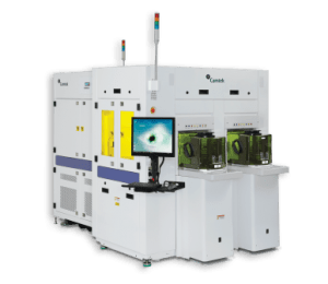
Products