Products
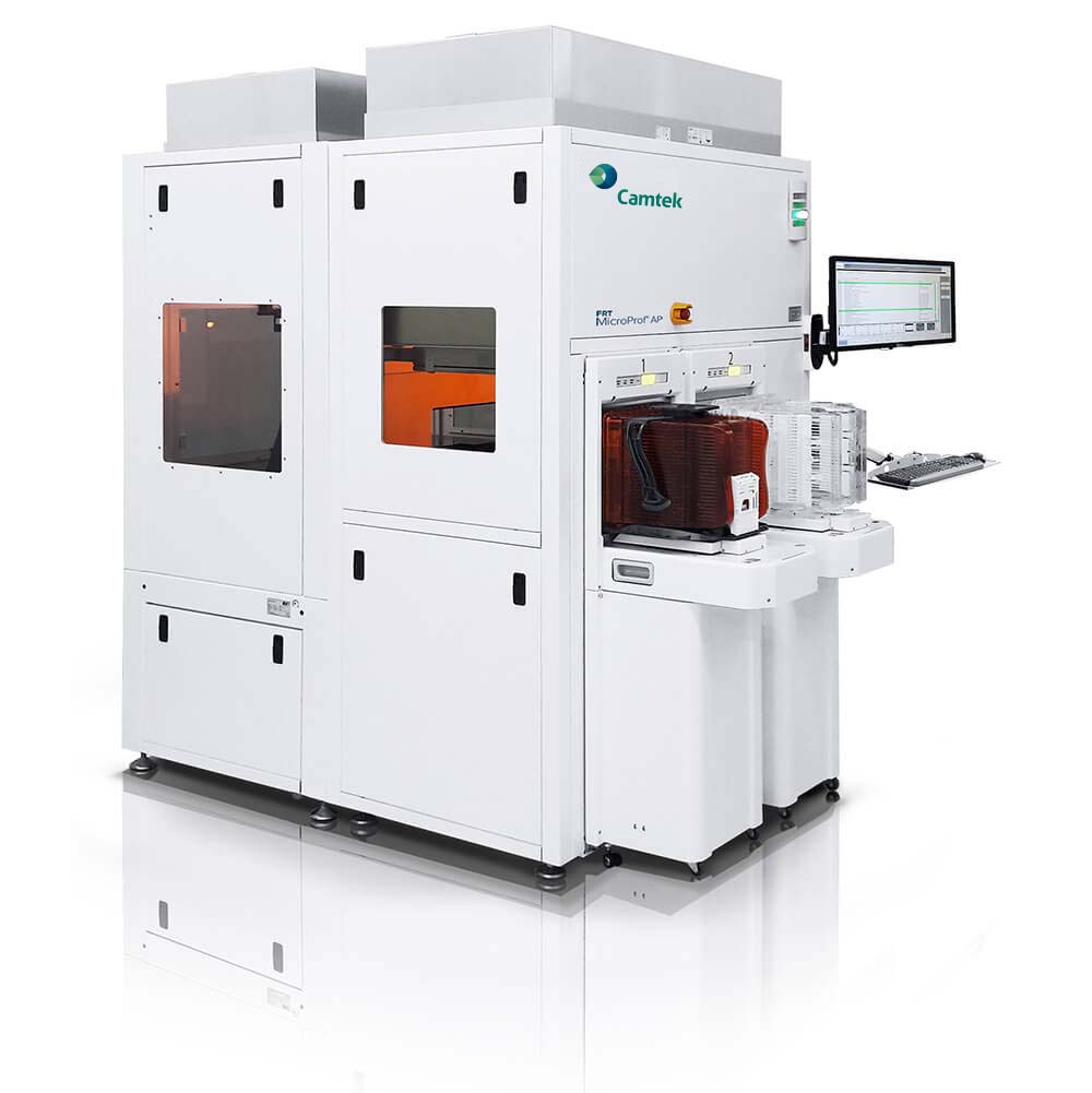
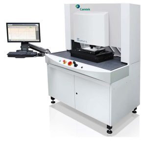
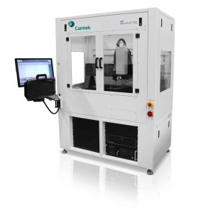
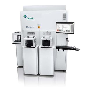
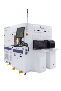
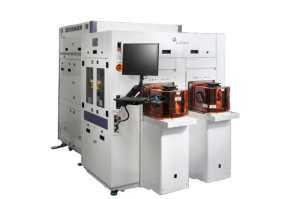
MicroProf® AP
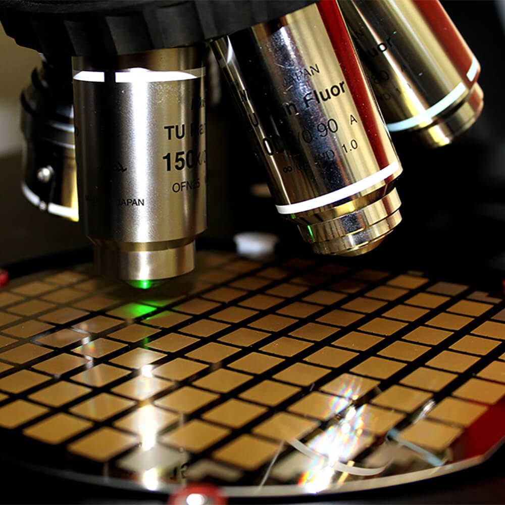
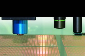
The FRT MicroProf® AP is a fully automated wafer metrology tool for a wide range of applications at different 3D packaging process steps, e.g. for the measurement of photoresist (PR) coatings and structuring, through silicon vias (TSVs) or trenches after etching, μ-bumps and Cu pillars, as well as for the measurement in thinning, bonding and stacking processes. With its modular multi-sensor concept, the flexible MicroProf AP measuring tool is ideally suited to perform a variety of measuring tasks in advanced packaging.
The FRT MicroProf AP also provides comprehensive measurement solutions for backside processing (backgrinding, metallization) for power semiconductors such as MOSFET or IGBT, as well as for the control of different substrates, e.g. bulk Si, SOI, cavity SOI, compounds such as GaAs, InP, SiC, GaN, ZnO, and also for transparent materials. Furthermore, it can be used for hybrid bonding and Micro Electro Mechanical Systems (MEMS), included in consumer electronics, automotive, telecom, medical and industrial markets.
Highlights
- Flexible multi-sensor metrology tool for advanced packaging
- For every process step from TSV etching, RDL/UBM/bumping to Cu nail reveal, dicing, stacking, and molding
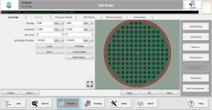
- Wafer handling unit with SEMI-standard FOUPs/FOSBs and open cassettes
- Individual configuration for your specific applications
- Retrofit on demand
Products
Acquire Automation XT
Easy recipe creation, multi-sensor measurement or hybrid metrology
Learn More >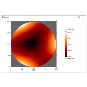
Mark III – Measurement Analysis SW
Process, evaluate, and present 2D or 3D measurements
Learn More >
360°Scan
Designed as a modular, add-on module to both the Eagle and the Hawk platforms.
Learn More >